E-mail: cysi@cysi.wang


The working principle of the reactive ion etcher (RIE) is based on the ionization reaction, which uses a high frequency electric field to produce a glow discharge of the reactive gas to form a plasma

The working principle of the reactive ion etcher (RIE) is based on the ionization reaction, which uses a high frequency electric field to produce a glow discharge of the reactive gas to form a plasma. The active ions in the plasma react physically and chemically with the etched material to achieve etching.
Application
Reactive ion etcher is widely used in microelectronics, nanotechnology, bioengineering, optics and other fields. Its high accuracy and wide material adaptability (from metal to insulating materials, from single crystal to polycrystal, from flat to three-dimensional complex shapes) make it widely used in scientific research institutions, university laboratories and high-tech companies.
Purchase information
If you are interested in our evaporation coater, please contact us for more information.
Tel:138 3857 9492
Email:carol@cysitech.com
Contact:Carol Xu
Wechat:15290599353
WhatsApp/Skype: 13838579492
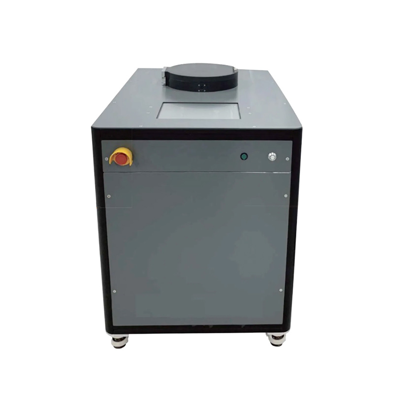
Technical parameters
Product name | Reactive Ion Etcher (RIE) | |
Product model | CY-RIE-100 | CY-RIE-200 |
Sample size | 4inch and below | 8inch and below |
RF power source | 0~300W/500W/1000W adjustable, automatch | |
Molecular pump | No/620(L/s)/1300(L/s)/Customized | |
Backing pump | Mechanical pump/dry pump | |
Process pressure control | No control pressure /0~1Torr control pressure | |
Gas type | H2/CH4/O2/N2/Ar/SF6/CF4/ CHF3/C4F8/NF3/Customized (Up to 9 channels: free of corrosive and toxic gases) | |
Gas range | 0~5sccm/50sccm/100sccm/200sccm/300sccm/500sccm/Customized | |
LoadLock chamber | Yes/No | |
Sample temperature control | 10℃~RT/-30℃~100℃//Customized | |
Chamber wall temperature control | No/RT~60/120℃ | |
Control system | Fully automatic/Customized | |
Dimensions | L1400mm*W800mm*H1080mm | |
Weight | ~300KGS | |
Case: Pattern transfer in semiconductor manufacturing
Purpose:
Transfer the photolithography pattern to the silicon oxide film on the silicon wafer through RIE technology, remove the silicon oxide in the non-pattern area, and form a fine microstructure.
Required equipment and materials:
Reactive ion etcher (RIE)
Silicon wafer (containing silicon oxide layer)
Photoresist (e.g., positive photoresist)
Photolithography machine (for exposure)
Developer (for development)
Etching gas: Usually a gas mixture such as oxygen (O2), fluorinated gas (such as SF6, CF4) is used.
Vacuum pump system (for maintaining a vacuum environment)
Operation steps:
1. Prepare silicon wafer
Wafer cleaning: Use deionized water, isopropyl alcohol (IPA) and other solvents to clean the surface of the silicon wafer to remove dust and contaminants. Ultrasonic cleaning can be used to ensure the cleanliness of the silicon wafer surface.
Dry silicon wafer: Blow the cleaned silicon wafer dry with nitrogen.
2. Apply photoresist
Photoresist coating: Apply photoresist evenly on the surface of the silicon wafer. The photoresist is usually applied using a spin coater to ensure that the coating is uniform and free of bubbles.
Soft bake: The photoresist-coated silicon wafer is placed in an oven or hot plate for soft baking (about 90-110°C for 1-2 minutes) to remove the solvent in the photoresist.
3. Exposure
The photoresist-coated silicon wafer is placed in a photolithography machine for exposure. During exposure, ultraviolet (UV) light is used to irradiate the photoresist surface, and the desired pattern is transferred to the photoresist layer through a mask.
The exposure time depends on the type of photoresist and the exposure intensity.
4. Development
Development treatment: The exposed silicon wafer is immersed in a developer, which is selected according to the type of photoresist (positive or negative). For positive photoresists, the exposed area will be removed by the developer, leaving the unexposed area.
The development time and temperature need to be adjusted according to the requirements of the photoresist to ensure a clear and complete pattern.
5. Hard bake
Hard bake: The developed silicon wafer is hard baked, usually at 120-150°C for 30-60 minutes. Hard bake helps to cure the photoresist and increase the mechanical strength of the photoresist.
6. RIE reactive ion etching
Loading silicon wafer: Place the processed silicon wafer into the etching chamber of the RIE etcher.
Set etching parameters:
Select appropriate reactive gas (e.g., O2, SF6, CF4, etc.).
Set working pressure (usually 10-50 mTorr).
Set RF power (usually 100-300 W), which is used to generate ion beams.
Set etching time (depending on film thickness and required etching depth).
Start etching: In the RIE machine, the reactive gas is excited by the electromagnetic field and RF power to form plasma, and the ions react with the gas to produce ionized etching substances. During the etching process, ions bombard the surface of the material and remove the silicon oxide under the photoresist.
Selective etching: RIE etching is highly selective and can only etch the material under the photoresist without damaging the photoresist pattern above.
7. Photoresist removal
After etching, use a stripping solution (such as acetone or N-Methyl-2-pyrrolidone, NMP) to remove the photoresist.
Wash to remove the remaining photoresist and wash again with deionized water and isopropyl alcohol.
8. Post-processing and inspection
Wash and dry: Use deionized water to wash the silicon wafer surface and then blow dry with nitrogen.
Inspection: Check the etched pattern through an optical microscope or scanning electron microscope (SEM) to ensure the accuracy of the pattern and the etching depth.
Summary:
Through the above steps, reactive ion etching (RIE) successfully transfers the pattern of the photoresist to the silicon oxide layer on the silicon wafer, removes the non-patterned area, and forms a high-precision microstructure. This process is crucial in semiconductor manufacturing and is widely used in the manufacture of integrated circuits, microsensors, MEMS devices, etc.


Copyright © Zhengzhou CY Scientific Instrument Co., Ltd. All Rights Reserved Update cookies preferences
| Sitemap | Technical Support: